
How Does PCB Manufacturing Assembly Accommodate For Torsional Stress?
- Posted on April 30, 2024
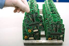
PCB Manufacturing Assembly Accommodate
In pcb manufacturing assembly, it’s necessary to accommodate for torsional stress. To do this, the assembly process must be monitored closely and controlled using statistical process control (SPC) tools. These ensure that all critical input factors are operating within defined control limits, preventing defects such as warpage and flexure. In addition, proper handling and packaging techniques must be employed to prevent damage in transit.
The pcb manufacturing assembly process is complex and multifaceted, leaving many opportunities for error. For example, temperature changes lead to expansion and shrinking of the board, resulting in warpage, which can interfere with device function and integrity. Other issues that may arise during PCB fabrication include component misalignment and poor solder joints.
To prevent these problems, a thorough inspection of the board must take place after it passes fabrication. In addition, the contract manufacturer should establish DFM (design for manufacturing) rules that address the specific requirements of the customer. Once the PCB passes inspection and is ready for assembly, it’s loaded into a pick-and-place machine. This robotic device receives the components from feeder reels and high-speed heads that move to accurately place them in their correct positions on the board.
How Does PCB Manufacturing Assembly Accommodate For Torsional Stress?
This is a time-consuming and labor-intensive process, but it’s essential for ensuring the correct placement of all components. A missed component can cause a failed circuit, so it’s important to have an in-line inspection system that checks each component to make sure it’s in its correct position on the PCB.
Another important inspection step is to evaluate the quality of the solder paste deposit. This is done by inspecting the pads for signs of overfilling and voids in the area around each component. Overfilling can result in poor solder bonding and a defective connection, so the inspection should be performed in a timely manner.
Next, the board is ready for layer alignment and optical inspection. The holes from the previous stage are used to line up inner and outer layers, ensuring all features are aligned properly. After the optical inspection is complete, the board undergoes final testing, confirming it meets all required specifications.
A faulty solder joint is an obvious issue, but torsional stress on a PCB can also cause other problems. For instance, it can cause delamination, cracking, and mechanical stress during handling or installation. In these cases, a torsional stress formula must be applied to determine the maximum value of force that can be applied to the object.
The most effective way to prevent torsional stresses during PCB assembly is to ensure all production processes are operating at the highest levels of efficiency and accuracy. This requires careful evaluation of the critical input factors that influence quality. Statistical process control (SPC) tools can be used to track and monitor these factors, making it easier for CMs to identify and correct errors in the assembly process. This helps to improve the quality of the finished product and reduce the likelihood of a malfunctioning or defective electronic assembly.
PCB Manufacturing Assembly Accommodate In pcb manufacturing assembly, it’s necessary to accommodate for torsional stress. To do this, the assembly process must be monitored closely and controlled using statistical process control (SPC) tools. These ensure that all critical input factors are operating within defined control limits, preventing defects such as warpage and flexure. In addition,…